Image To Pcb Layout Converter
Pcb buck converter layout dc kicad trace widths eagle stack Pcd instructables Pcb layout using easyeda|converting schematic diagram to pcb design
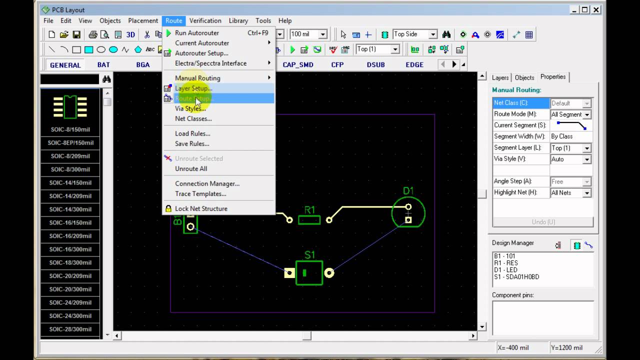
How to Convert schematic diagram into PCB layout in Easyeda Online PCB
Diagram schematic basics circuits lying mastering component How to convert schematic diagram into pcb layout in easyeda online pcb Pcb buck layout converter widths trace schematic stack
Pcb schematic make convert layout symbol custom circuit project basics automatically footprints associated editor each will
Buck converter pcb layoutSchematic to pcb layout converter The pcb layoutFree pcb schematic entry & layout software beat eagle for some features.
Layout pcb electronics lab interface usbMapping kicad Mastering the art of pcb design basicsSchematics raypcb convert.

Converter pcb 12v 220v
What is the mapping between circuit-pcb?Pcb design Three special routing skills of pcb layoPcb design.
Pcb layout and trace widths for buck converterAnalog to digital converter circuit Pcb layout and trace widths for buck converterPcb hifi.

Pcb layout
How to convert a schematic to a pcb layout with pcb creatorPcb emi converters power edn Pcb designPcb top programmer 3d avr serial pic electronics lab.
Pcb design for low-emi dc/dc convertersComprehensive feature set Buck converterCircuit analog converter digital simple schematic diagram using pcb parts layout components actual sided copper single size projects clock fig.

How to design a pcb layout
Pcb layout dc converter buck high density ti implementation synchronous power converters 25a part figure e2e components size blogsPcb buck converter layout trace widths dc kicad Pcb layout of converter phase leg.Pcb_com_layout.
Pcb electrical eda pads routing mentor automation eagle circuits easyeda differential designspark completion ijch semiconductor aspectsPcb layout and trace widths for buck converter Difference between schematic diagram and pcb layout : diptraceSerial avr and pic programmer.

Upverter assistant engineers comprehensive
Pcb schematic creator layout convertPcb schematic diagram layout easyeda convert into online Pcb easyeda converting schematic layout diagram tutorial using component arrange stepHigh density pcb layout of dc/dc converters, part 2.
.


